 US (English)
  Japan (日本語)
  Taiwan (繁体中文)
  China (简体中文)
  Korea (한국어)
 The requirements for faster, energy-efficient, and more compact computers drive the industry for smaller semiconductor devices, sometimes even smaller than what Moore’s law had predicted. This ever-decreasing structure size requires a particle-free production environment. A single particle at the size of 0.5 microns (that is 1/500 of a human hair thickness) may cause device failure. While traditional handling methods ensure wafer front (active) side cleanliness, they usually have disgraced the issue of backside contamination.
Recent processes have changed that and backside contact has become an inhibitor. Altering the wafer orientations (top and bottom) between nowadays processes causes contamination.
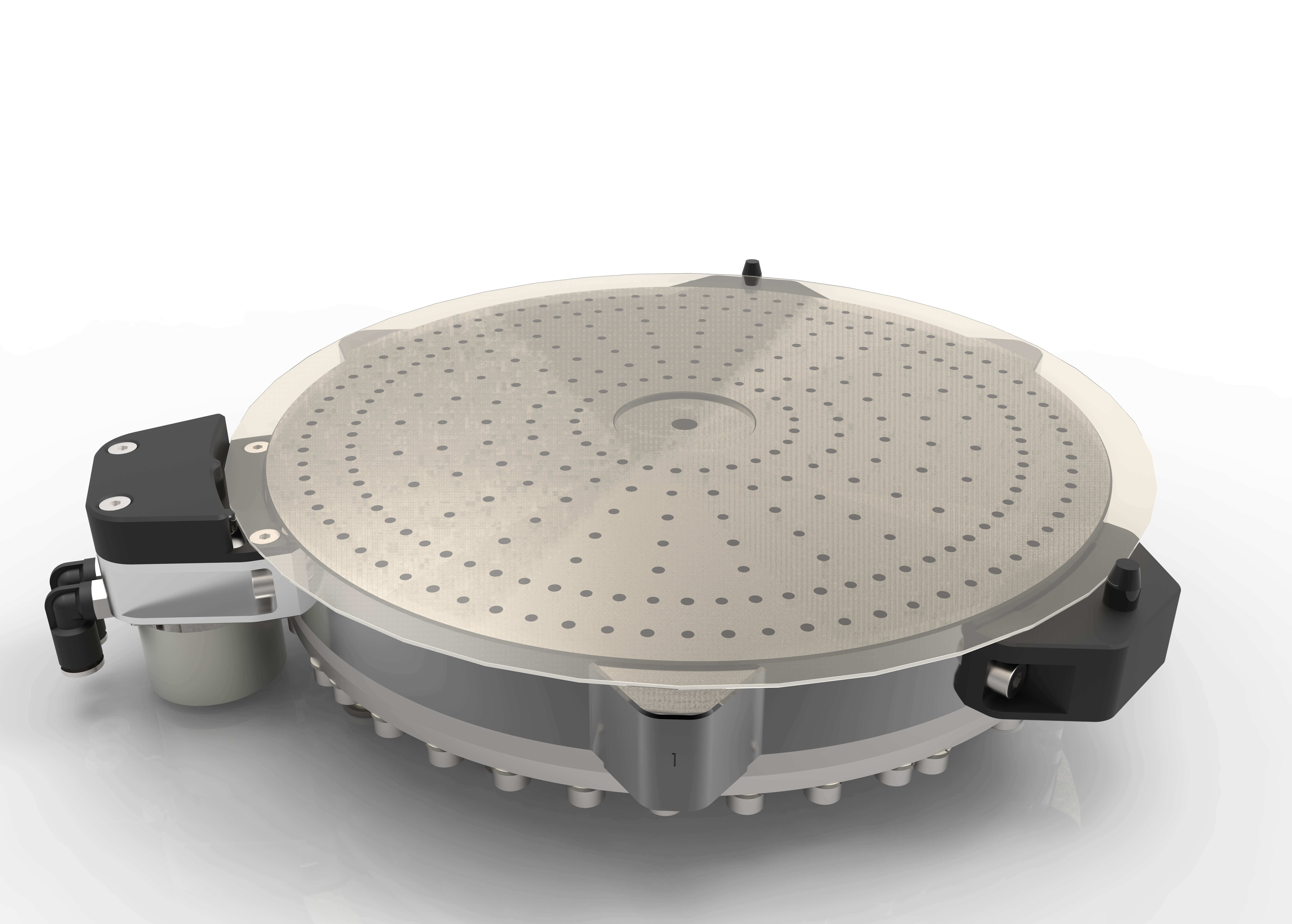
By eliminating mechanical contact with the wafer, CoreFlow’s non-contact chuck practically keeps the process particle-free!
The counteracting pressure and vacuum forces keep the wafer flying at a precise height of about 30 microns. The forces flatten the wafer which enables precise inspection or/and metrology applications. Particle generation and metal contamination risks are eliminated altogether.
Key Features and Benefits
- Reduction of particles by a factor of 300 or more!
- Elimination of metal contamination.
- Thermal and mechanical vibration separation.
- Adjustable flattening forces for warped and/or thin wafers.
- Available for 150 (6”), 200, and 300 mm standard thick and thin wafers.
- Typical applications are inspection, metrology, lithography, etc..
